MPPT Solar Charge Controller
MPPT Solar Charge Controller
The idea for an MPPT solar change controller (MPPT Solar CC) first came about as when I was building my Hydroponic system. Given that I wanted to power at least the lights from solar energy, I began doing some research on solar arrays and how best to set up my system. This was where I chanced upon the idea of MPPT and how it could save up to 30% more power from my solar panels, something very desirable since I only had so much space and thus a very limited number (1) of solar panels at my disposal.
I initially found a variety of solar charge controllers available on the market, however unfortunately they were either fake MPPT or pretty expensive (I narrowed down on the EPever Tracer modules and they start at SGD$60 for 10A). Given this, as well as the hope that I could make the CC “smart” through integration with WiFi logging (which would fit into the whole smart home initiative I had), I decided to try my hand at making a MPPT charge controller from arduino components.
The initial phase saw me doing extensive research on how to control the charging circuit of the solar charge controller. I vaguely knew that it would be along the lines of a DC-DC switch mode power supply (SMPS) but due to a general lack of knowledge in this aspect, initial trials to design my own SMPS from scratch (ie to size all the components and build the circuit wasn’t very successful… [As in it worked but it wasn’t consistent and reliable]). Hence to save me some time before I actually got down to study SMPS, I decided to integrate an existing SMPS circuit into my design, saving me time in ironing out the switching aspect. I set about looking for a relatively low-cost, arduino controllable SMPS unit, and soon stumbled across the LTC3780 Synchronous Buck Boost Converter sold under the designation of WD2002SJ from online Chinese suppliers like Aliexpress or Banggood. This board has the following specs:
- Input Voltage Range: 5V - 32V
- Output Voltage Range: 1V to Input voltage + 5 to 6V
- Output Current: 10A max, 7A sustained
- Output Power: 80W sustained, 100W peak (I am sure the spec sheet has a typo in it)
These specifications were retrieved from the aboved datasheet.
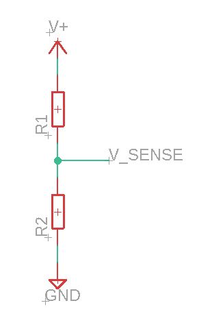
The new problem was that now I needed some way to control the Converter. As an amateur I spent some time studying the topology of the board and learnt that the potentiometer that controlled the voltage was such that the wiper was connected to a voltage sense pin which would by working of “some op amps” in the circuit, always maintain a voltage of 0.8V between itself and ground (as per the circuit diagram below).
Thus, we can derive a mathematical equation that would give us the output voltage based on the input voltage.
Since the voltage across V_Sense and GND is always at 0.8V (measured wrt GND), asuuming that there is no input from a microcontroller, the voltage across the output (V_Out) and V_Sense cacn be modelled using the voltage divider equation:
\[\ V_{Sense} = V_{Out} * \frac{R_2}{R_1+R_2}\]Rearranging yields:
\[V_{Out} = V_{Sense} * \frac{R_1 + R_2}{R_2}\]However, by adding a resistor \(\ R_3\) and applying a voltage at V_Sense, V_out can now be controlled by varying the voltage through a micro-controller analog pin. Given new setup is represented by the circuit diagram below:
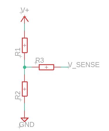
By considering current flowing through resistors, we obtain the following expression for current through \(\ R_3\):
\[\ I_{R_3} = \frac{V_{Sense} - 0.8}{R_3}\]We assume that positive current represents current flowing from \(\ V_sense\) into \(\ R_3\)
Current through \(\ R_2\) is given to be:
\[\ I_{R_2} = \frac{0.8 V}{R_2}\]This is because we know that the voltage across \(\ R_2\) is always 0.8V
Thus by Kirchoff’s First Law:
\[\ I_{R_2} = I_{R_1} + I_{R_3}\] \[\ I_{R_1} = I_{R_2} - I_{R_3}\]Thus given that \(\ V_{R_1} = I_{R_1} * R_1\)
\[\ V_{Out} = 0.8V + I_{R_1} * R_1\] \[\ V_{Out} = 0.8V + (I_{R_2} - I_{R_3}) * R_1\] \[\ V_{Out} = 0.8V + (\frac{0.8 V}{R_2} - \frac{V_{Sense} - 0.8}{R_3}) * R_1\]Thus, we derive the following mathematical relationship between the output voltage, \(\ V_{Sense}\) and \(\ R_1, R_2\) and \(\ R_3\). The main article from which these relationships are derived from can be found here. To solve for the values of each resistor, I used Desmos to graph the relationship between \(\ R_1, R_2\) and \(\ R_3\) for the logic level the arduino was configured to (5V). As such, I obtained the following values for \(\ R_1, R_2\) and \(\ R_3\):
\(\ R_1\) : 250K \(\ R_2\) : 14K \(\ R_3\) : 220K
These values were obtained purely through playing around with the sliders in the Desmos graph to determine the optimum set of values that would give me my desired range of output voltages given the range of input voltages from 0-5V.
The input voltage for controlling the voltage was supplied by means of a MCP4725 Digital Analog Converter (or DAC) as I the ATMEGA2560 (as with most Arduino boards) does not have a Digital Analog Converter.
After sorting out the voltage regulation bit, it was then time to sort out the voltage and current sensing part of this project (after all, we have to know what the value of the voltage and current of our panels and battery is to make any attempt at being a charge controller)! To that end, I turned to a specialized IC - the INA219 which is an variable-precision power monitoring IC that is capable of measuring both voltage and current through a shunt resistor. Using an appropriate value of shunt resistor, I was thus able to obtain values for both current and voltage in the desired range.
From the Adafruit Product Page,the maximum voltage across the voltage sense bus was +26V, more than enough for our application of measuring up to 18V (solar panel OC Voltage). The current measurement threshold was calculated from the maximum differene in voltage between the input sense pins for the shunt resistor which is \(\ \pm 320 mV\). Thus, given a resistor of \(\ 0.1 \Omega\), the maximum current through the shunt was calculated according to Ohm’s Law:
\[\ I_{max} = frac{\pm 320 \times 10^{-3}}{0.1 \Omega}\]Which yields 3.20 V.
In order to increase the current measurable through the sensor, the shunt resistance value had to be increased as per the above equation. Thus, the maximum current measurable was increaed tenfold by selecting a 10 times smaller resistor (\(\ 0.01 \Omega\)) which allowed for current measurement up to \(\ \pm 32A\) (way above our requirements). However, a noteworthy tradeoff was the decreased resolution of the current reading (which also increased tenfold to \(\ \pm 8mA\)). However, given the nature of the currents being measured, this decrease in resolution was not a concern.
After all the dust had settled with the core components of the controller, it was now time to focus my attention to the reason why I even bothered doing this in the first place - WiFi logging and remote monitoring of the charge controller! To serve this role, I chose to use an ESP32 board solely due to the fact that I had experience in working with this low-cost module and it was also readily available as a WiFi option at the time of writing. To save space on my already densely populated board and also because I was already using a dedicated microcontroller to handle the heavylifting of the calculations, I configured the ESP32 as a mere serial slave that would simply communicate with the microcontroller via AT commands, something which necessitated the use of either a software serial or a dedicated hardware serial port. This was hence a very large consideration that led me to choose the ATMEGA2560 as the microcontroller of choice.
Now that most of the key components were settled, it was time to start prototyping. As always, I started prototyping on breadboard before moving on to manufacturing a PCB (speaking of which it was an exhilirating experience for me as it was my first time ordering a PCB from a fab house)! I initially encountered every single problem you could think of - from poor breadboard connections (most annoying) to general issues with the libraries and code (there exist so many INA219 libraries and I’ll provide the code for those which worked). The most annoying of all issues however, was that the voltage regulation would sometimes yield inconsistent results and wildly inaccurate results. The final value of the resistor \(\ R_3\) (150K) which worked for me differed from the theoratical value by so large an amount that it was almost as if the theory did not exist (oops).
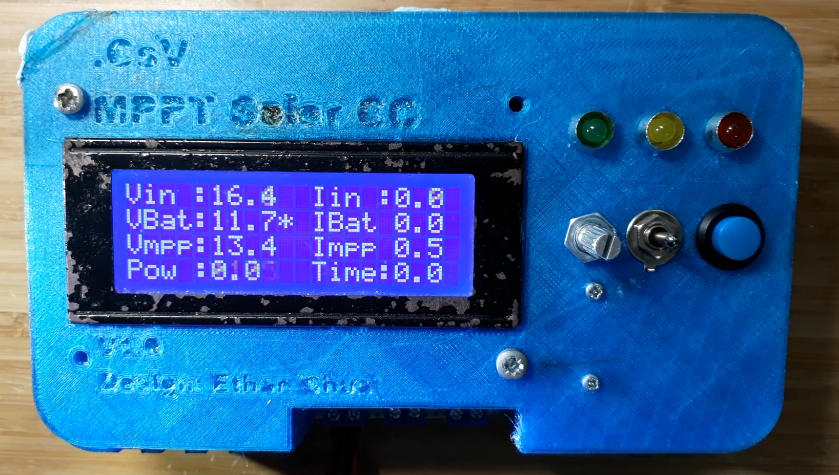
After the key components showed some semblance of working, I proceeded to add on the bells and whistles, namely auxillary features such as SD card logging, a Graphical User Interface (GUI) complete with a rotary encoder. The final product also includes LED display lights to quickly convey critical information such as presence of SD card / undervoltage etc.
The GUI was unexpectedly difficult to code, since it required me to think in a way that I had never done before - by emulating the behavoir of a GUI! For the first time I was considering the screens of the GUI screen by screen and having to map out the exact position of each of the elements and ensuring that the cursor position never accidentally wiped out what was not meant to be wiped (because the LCD library uses print as the display function). Moreover, my initial poor programming knowledge (yes this project is very old and has undergone extreme revamping) decided that it was a good idea to use while(true) and break; to keep the UI at a particular screen, a tragic mistake that caused me to have to redo the entire code with variable states for each screen instead. (Full code is linked at the end) The very large size of the sketch file at the end of the day prompted me to choose the ATMEGA2560 as a microcontroller, a move which on hindsight seems extremely bizarre and over-cautious, given that the sketch now only uses up 42986, bytes (16%) of it’s memory space, making me wonder if I should have used something more appropriate like an ATMEGA328P or even an ATTINY24A with SoftwareSerial to emulate a serial port for the ESP32.
Needless to say, I designed the board in Autodesk EAGLE and sent it to the fab house for production, yay!
Soldering the components onto the board was another epiphany for me as it formally introduced me to the world for SMD soldering and showed me how easier it actually could be. I tried and busted a board trying to manually solder SOT-23 chips (a very silly move) and this thus forced me to learn how to SMD solder with solder paste, something that still fills me with awe till this day. Soldering the parts was still a massive pain even with the soldering paste, as the tiny footprint meant that contact between the pads and the pins was often quite weak and inconsistent. I would often have an I2C scan fail to recognize a bunch of components on the board, only for them to show up when I re-soldered them on. This thus would prove a real pain throughout the development of this product.
Once everything was done, it was time for putting everything together. To house all the circuitry, I designed a 3D printed case in AutoDesk Fusion360 which incorporated a simple friction fit lid to keep everything inside as well as mouting holes for the 16 x 4 lCD and the display LEDs, buttons, switches and rotary encoder.
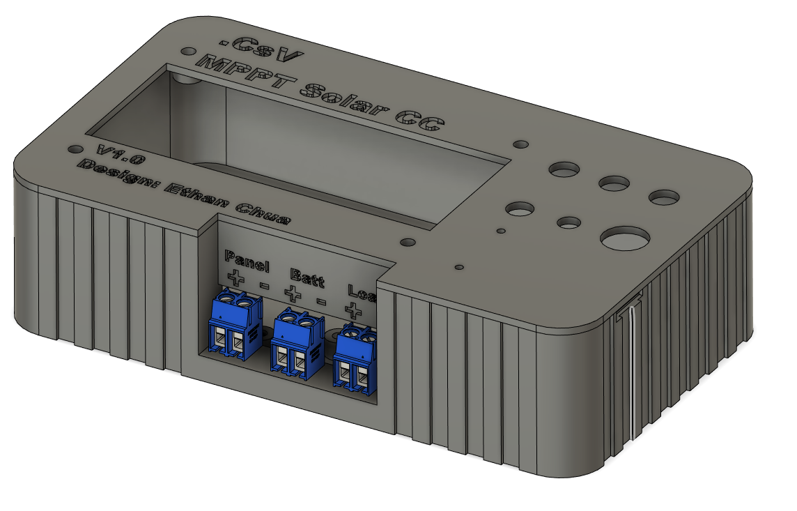
The final product looks something like this:
The MPPT algorithm was implemented by a simple “hill-climbing” algorithm which takes the following steps:
- Measure power generated by the solar panel
- Perturb the voltage across the solar panel in either the positive or negative direction (by design this is positive at the start)
- Measure the power again
- If there is an increase in the power, proceed to adjust the voltage across the panel in that direction
- Repeat until the voltage oscillates around a stable point which would be maximum power point.
Although this method for adjusting voltage was not the most foolproof method (given that firstly there is there no method to reflect the degree of error from the “true” value and the current value [as the “true” value of the voltage is not known] and secondly, that the correction adjustment is not-proportional to the magnitude of error [once again because there is no “true” value of the voltage]).
This method has seemed to work fine, although testing was very limited due to early failure of the DAC which resulted in me having to order another one…
As promised the sources files are linked here
Future Updates: In the future I would definitely want to design the entire switching circuit on one board rather than try to connect various components across boards as this would greatly simplify the design process. Moreover, further research should be done on the MPPT algorithm (perhaps incremental conductance algorithm or a gradual decreasing of the value of the error adjusting variable as the voltage value begins to oscillate). I will continue working on this project as I think that it has good potential not just for the sake of a fun project that has exposed to to SMD soldering, but also as a useful product I hope will allow more end-users to get into the realm of solar energy.